In this article:
- Introduction
- DDR5 V's DDR4 Comparison
- DDR5 Scales to 8.4 GT/s
- Lower Voltage Keeps Power Manageable
- New Power Architecture for DDR5 DIMMs
- DDR5 vs DDR4 Channel Architecture
- Longer Burst Length
- A Smarter DIMM with DDR5
- DDR5 Supports Higher Capacity DRAM
- What are the DDR5 Design Challenges?
- How Do DDR5 Memory Interface Chipsets Harness The Advantages of DDR5 For DIMMs?
- DDR6 RAM Now In Development
- When Is DDR6 Coming?
- What Can We Expect From DDR6 RAM?
- DDR6 Is the Future
Introduction
Intel’s 12th Generation Chips (Alder Lake) and 13th Generation Chips (Raptor Lake), are engineered to support DDR5 memory. The advent of these cutting-edge memory modules has ushered in a new era for industrial systems, soon to be embraced by computers worldwide. DDR5 has astounded users with its remarkable speed, surpassing even the swiftest DDR4 kits.
With each RAM iteration, enhanced speed naturally follows as a staple improvement, complementing other advancements between generations. While RAM performance encompasses more than just frequencies, DDR5 stands out with its exceptional velocity. The initial DDR4 memory modules commenced at 2133 MHz and gradually reached 3600 MHz, albeit with a premium for higher-end kits.
In contrast, DDR5 revolutionises the landscape with a doubled base frequency. Starting at an impressive 4800 MHz, current kits have already scaled up to an astonishing 6400 MHz, signifying a monumental leap in RAM speed.
But the excitement doesn’t end there. Future projections envision DDR5 surging to unprecedented heights of 8400 MHz, a figure that currently defies imagination. And who can say if innovation will push the boundaries even further beyond this remarkable threshold.
DDR5 V's DDR4 Comparison
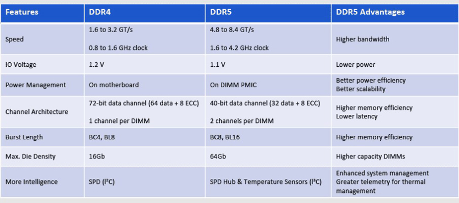
The following outlines the top significant specification upgrades, summarised in the following table:
DDR5 Scales to 8.4 GT/s
DDR4 DIMMs peaked at 3.2 giga transfers per second (GT/s) with a clock rate of 1.6 gigahertz (GHz), the initial DDR5 DIMMs astound with a remarkable 50% surge in bandwidth, soaring to an impressive 4.8 GT/s. But the journey doesn’t stop there — brace yourself for the future as DDR5 memory transcends boundaries, scaling up to an astounding data rate of 8.4 GT/s.
This ground-breaking achievement in performance is made possible by incorporating innovative features like Decision Feedback Equalization (DFE), which empowers DDR5 to achieve higher IO speeds and data rates. Prepare to embrace a new era of unparalleled memory performance with DDR5.
Lower Voltage Keeps Power Manageable
A second major change is a reduction in operating voltage (VDD) and that helps offset the power increase that comes with running at a higher speed. With DDR5, the DRAM, the registering clock driver (RCD) voltage drops from 1.2 V down to 1.1 V. Command/Address (CA) signalling is changed from SSTL to PODL, which has the advantage of burning no static power when the pins are parked in the high state.
New Power Architecture for DDR5 DIMMs
DDR5 DIMMs incorporate a power management IC (PMIC) on the DIMM module itself, operating at 12 volts. This advancement enables enhanced precision in distributing system power loads. The PMIC facilitates the distribution of the 1.1-volt VDD supply, leading to improved signal integrity and reduced noise. Moreover, it offers superior on-DIMM control over the power supply, resulting in more efficient power management.
DDR5 vs DDR4 Channel Architecture
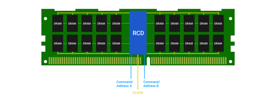
Discover the game-changing innovations of DDR5, including a significant transformation in DIMM channel architecture, securing its spot as the fourth major change on our list. Unlike DDR4 DIMMs with a 72-bit bus consisting of 64 data bits and eight ECC bits, DDR5 introduces a revolutionary approach. Each DDR5 DIMM is equipped with two channels, enhancing efficiency and memory access. Each channel boasts a 40-bit width, comprising 32 data bits and eight ECC bits. This architecture not only maintains a total data width of 64 bits but also amplifies the benefits of DDR5’s speed advancements through improved efficiency.
In the DDR5 DIMM architecture, the left and right sides of the DIMM operate independently, with each side served by a dedicated 40-bit wide channel. Additionally, DDR5 elevates performance by enhancing the Registered Clock Driver (RCD) functionality. Unlike DDR4, where the RCD provides two output clocks per side, DDR5 empowers the RCD to deliver four output clocks per side. This advancement proves especially advantageous in the highest density DIMMs featuring x4 DRAMs. Each group of five DRAMs, constituting a single rank and half-channel, receives its independent clock. This strategic enhancement not only improves signal integrity but also effectively addresses the challenge of lower noise margin resulting from the reduction in VDD as discussed in the second change.
Embrace the extraordinary advancements of DDR5, where enhanced DIMM channel architecture and clock distribution work synergistically to redefine memory performance and propel your computing experience to new heights.
Longer Burst Length
While DDR4 boasts a burst chop length of four and a burst length of eight, DDR5 takes it to the next level. DDR5 extends both burst chop and burst length to eight and sixteen, respectively, delivering an exponential boost to burst payload capacity. The introduction of a sixteen-burst length (BL16) enables a single burst to access a substantial 64 Bytes of data, aligning perfectly with the typical CPU cache line size. Astonishingly, this feat is accomplished using only one of the two independent channels. The result? A significant enhancement in concurrency and with the added advantage of dual channels, unparalleled memory efficiency.
A Smarter DIMM with DDR5
The DDR5 server DIMM chipset introduces several advancements over DDR4, including the replacement of the DDR4 SPD IC with an SPD Hub IC and the addition of two temperature sensor (TS) ICs. This upgrade allows for enhanced thermal monitoring and management within the RDIMM module.
With DDR5, the communication bus between chips undergoes a significant improvement by transitioning to I3C, which operates at a speed ten times faster than the previous I2C bus used in DDR4. The DDR5 SPD Hub facilitates communication between the module and the Baseboard Management Controller (BMC). Leveraging the faster I3C protocol, the DDR5 SPD Hub significantly reduces initialisation time while enabling a higher rate of polling and real-time control.
The thermal information gathered by the SPD Hub is transmitted to the BMC, offering valuable data for effective cooling fan speed management. Additionally, the DDR5 technology allows for more precise control over the DRAM refresh rate, enabling higher performance or better data retention. If the RDIMM temperature exceeds optimal levels, the bandwidth can be adjusted accordingly to mitigate the thermal load.
Overall, the DDR5 server DIMM chipset’s incorporation of the SPD Hub IC, temperature sensor ICs and the improved I3C communication bus ensures better thermal monitoring, faster initialization, and enhanced control for optimal performance and temperature regulation.
DDR5 Supports Higher Capacity DRAM
One significant enhancement to emphasise is DDR5’s capability to accommodate higher-capacity DRAM devices. By employing DDR5 buffer chip DIMMs, server and system designers gain the ability to incorporate densities of up to 64 Gb DRAMs within a single-die package.
In comparison, DDR4 is limited to a maximum of 16 Gb DRAMs in a single-die package (SDP). DDR5 introduces various features such as on-die ECC, error transparency mode, post-package repair, and read and write CRC modes, all geared towards supporting higher-capacity DRAMs.
The implications of these higher-capacity devices are evident in the increased capacity of DIMMs. While DDR4 DIMMs can reach capacities of up to 64 GB using SDP, DDR5 SDP-based DIMMs go beyond that, quadrupling the capacity to an impressive 256 GB.
These advancements in DDR5’s support for higher capacity DRAM devices not only expand the memory capabilities of systems but also enable more efficient data processing and storage. By optimising the utilization of memory resources, DDR5 empowers server and system designers to meet the growing demands of modern applications and workloads, ultimately enhancing overall system performance and productivity.
What are the DDR5 Design Challenges?
The introduction of DDR5 brings forth a set of design considerations related to higher RAM speeds and lower voltages, ushering in a fresh set of challenges concerning signal integrity. Designers must ensure that both motherboards and DIMMs are capable of handling the increased signal speeds. System-level simulations should be performed to verify signal integrity at all DRAM locations.
In DDR4 designs, the primary focus of signal integrity challenges was on the dual-data-rate DQ bus, with relatively less attention given to the lower-speed command address (CA) bus. However, in DDR5 designs, even the CA bus demands special attention to maintain optimal signal integrity. While DDR4 incorporated differential feedback equalization (DFE) to enhance the DQ data channel, DDR5 necessitates DFE options for the RCD’s CA bus receivers as well, ensuring reliable signal reception.
The power delivery network (PDN) on the motherboard, including the connection to the DIMM with the PMIC, is another crucial consideration. Given the higher clock and data rates, it is essential to ensure that the PDN can handle the increased load of operating at higher speeds while maintaining excellent signal integrity and providing clean power supplies to the DIMMs.
Furthermore, the DIMM connectors that link the motherboard to the DIMM module must be capable of accommodating the new clock and data rates. System designers must place greater emphasis on electromagnetic interference and compatibility (EMI and EMC) in the system design, particularly with regards to the higher clock speeds and data rates present on the printed circuit board (PCB).
By addressing these design considerations related to signal integrity, power delivery, and EMI/EMC, DDR5 technology can be effectively harnessed to maximize system performance and ensure seamless operation in high-speed computing environments.
How Do DDR5 Memory Interface Chipsets Harness The Advantages of DDR5 For DIMMs?
DDR5 memory interface chips bring significant improvements to signal integrity, particularly for the command and address signals transmitted from the host memory controller to the DIMMs. Each channel’s bus is routed to the RCD (Registering Clock Driver) and then distributed to the two sections of the DIMM. This architecture effectively reduces the load on the CA bus, enhancing signal integrity and minimizing potential issues encountered by the host memory controller.
The expanded chipset, which includes the SPD Hub and TS, empowers smarter DIMMs capable of operating at higher data rates offered by DDR5 while still operating within the desired power and thermal limits. This advancement ensures that the DIMMs maintain optimal performance levels without exceeding designated power and thermal thresholds.
Numerous manufacturers now provide DDR5 memory interface chipsets, enabling designers to fully leverage the benefits of DDR5 technology while effectively addressing the challenges associated with higher data rates, CA signals, and clock speeds. With performance levels now reaching an impressive 6400 MT/s, these chipsets offer the necessary support for achieving exceptional performance and reliability in DDR5 memory systems.
By utilising these DDR5 memory interface chipsets, designers can ensure robust signal integrity, harness the enhanced capabilities of DDR5 and deliver outstanding performance in high-speed computing environments.
DDR6 RAM Now In Development
The continuous evolution of RAM remains a fascinating journey and as DDR5 gains prominence within the mainstream community, anticipation grows for the next advancement—DDR6 RAM. With faster speeds and the utilization of MSAP (Multi-Signal Access Point) technologies, DDR6 holds the promise of pushing the boundaries of memory performance even further.
But what exactly does this mean and how long can we expect DDR5 to dominate the spotlight? Let’s delve into the details. While specific release dates for DDR6 are yet to be confirmed, industry projections suggest that DDR6 RAM will make its debut in the near future. With this new iteration, we can anticipate even higher speeds and improved capabilities.
To fully embrace DDR6 RAM, certain requirements must be met. System architectures will need to support DDR6 technology and compatible motherboards and processors will need to be available. It’s important for users to keep an eye on hardware manufacturers’ announcements and specifications to ensure compatibility when DDR6 becomes available.
As for the duration of DDR5’s prominence, it is challenging to predict with absolute certainty. However, technological advancements in the memory industry typically follow a cycle, with each iteration enjoying a period of dominance before the next generation emerges.
DDR5 is still in its relatively early stages of adoption and it is expected to remain a prevalent memory standard for several years.
The advent of DDR6 RAM holds great promise for pushing memory performance to new heights. As the industry progresses, it is crucial to stay informed about release timelines, anticipated speeds and the hardware requirements necessary to fully leverage DDR6’s capabilities.
Exciting times lie ahead for RAM enthusiasts and we eagerly anticipate the arrival of DDR6 and the possibilities it brings.
When Is DDR6 Coming?
As of February 2023, DDR6 is confirmed to be in development, with Samsung announcing at its Tech Day that DDR6 is expected to arrive as modules for commercial use in 2025. With this in mind, this assures a fairly long lifecycle for DDR5 especially considering DDR6 will need to be integrated into RAM sticks before it can be used on a consumer level.
Remember that one of the reasons to upgrade your motherboard is so you can use DDR5 RAM.
What Can We Expect From DDR6 RAM?
DDR6 Speeds
As DDR RAM progresses through its iterations, a notable trend emerges—each new version tends to double the speeds of its predecessor. In the case of DDR5, it currently operates at a maximum data speed of 51.2 Gigabytes per second across two channels per module. However, it’s important to note that JEDEC modules typically offer speeds of 6,400MBps, with faster modules being released throughout the lifecycle of DDR5.
Looking ahead, DDR6 is poised to make its debut with impressive data rates. Projections indicate that JEDEC modules will achieve speeds of up to 12,800MBps, while overclocking can push those speeds even further to 17,000MBps. It’s worth noting that these speeds are expected to increase as the DDR6 lifecycle progresses.
It’s essential to remember that DDR is just one of the crucial terms to be familiar with when discussing RAM. The world of computer memory encompasses a range of concepts and technologies that contribute to overall system performance. Keeping abreast of these developments ensures a comprehensive understanding of RAM and its role in modern computing environments.
By staying informed about the advancements in DDR RAM speeds, particularly with the introduction of DDR6, enthusiasts can make informed decisions about their system’s memory requirements, maximizing performance and efficiency.
New Technology: MSAP
Samsung’s use of MSAP technology is increasingly prevalent in its DDR RAM modules, revolutionising the memory landscape. MSAP, which stands for Modified Semi Additive Process, has already found its way into certain DDR5 RAM brands. This cutting-edge technology enables manufacturers to design modules with finer circuits, unlocking the potential for higher speeds and enhanced connectivity.
By employing MSAP, manufacturers can effectively coat empty spaces within the circuits, optimising data transfers and bolstering connectivity between various components. This breakthrough innovation empowers DDR6 RAM modules to achieve faster speeds, contributing to improved overall system performance.
As MSAP continues to gain traction, the utilisation of this technology becomes a vital consideration when selecting DDR6 RAM modules. Manufacturers that implement MSAP can deliver enhanced circuitry, enabling users to harness the full capabilities of DDR6 and enjoy seamless computing experiences.
MSAP technology is set to play a crucial role in shaping the future of DDR6 RAM as by embracing MSAP-enabled DDR6 modules, users can unlock higher speeds, superior connectivity and ultimately, optimise their system’s performance for a wide range of computing tasks.
DDR6 Is the Future
While DDR6 is still in its early stages, with finalisation expected within approximately a year and commercial release anticipated in two years, the wait will be well worth it. DDR6 brings forth a significant leap in performance, promising speeds that are double the current standard.
As the industry continues to advance, staying updated on the progress of DDR6 and its impending release will be essential for tech enthusiasts and system builders. Prepare to witness the remarkable improvements in memory speeds and the integration of cutting-edge technologies like MSAP, which will undoubtedly shape the future of computing performance.
